Advanced chips are often described as if they are simply smaller versions of older chips. In practice, they are closer to a tightly coupled industrial system in which every part of the stack depends on every other part. The result is a manufacturing problem with unusually few shortcuts: improving one layer often exposes a weakness in another.
That is why the question is not just whether a chip design can be made to work. It is whether a foundry can print it, connect it, test it, cool it, and do all of that at scale with acceptable yield. The hard part of advanced semiconductors is not any single step. It is the coordination problem.
Scaling is no longer a simple reduction in size
For decades, the industry lived on the assumption that making transistors smaller usually made chips faster, denser, and more power-efficient. That basic logic still matters, but it has become much more expensive and much less automatic. When a feature is measured in nanometers, tiny deviations in line width, placement, or material thickness can affect performance.
At older nodes, a chip design could tolerate more variation. At leading-edge nodes, that slack disappears. A transistor that is slightly too leaky, a wire that has slightly too much resistance, or a pattern that prints imperfectly can change how the entire die behaves. This is why semiconductor manufacturing is often compared to photography, printing, chemistry, and factory automation all at once—but with vastly less room for error.
EUV helps, but it does not eliminate the hard parts
Extreme ultraviolet lithography, or EUV, is one of the most important breakthroughs in modern chipmaking. It uses much shorter wavelengths of light than older lithography systems, allowing finer features to be printed with fewer patterning steps. In theory, that should simplify the process. In reality, EUV replaces one category of difficulty with another.
The machines are extraordinarily complex, expensive, and slow to deploy. They require tightly controlled environments, advanced optics, specialized resist materials, and extremely precise light sources. Even when the tool works as intended, the surrounding process window can be narrow. That means the chipmaker still has to solve for defect control, overlay accuracy, and yield across an entire wafer.
In other words, EUV is not a magic wand. It is an indispensable tool in a manufacturing chain that remains fragile by design.
Yield is the economic gatekeeper
One of the most overlooked realities in chipmaking is that a chip is not valuable merely because it can be fabricated. It is valuable because enough copies of it can be fabricated correctly. That is the difference between a successful tape-out and a profitable product.
Yield refers to the percentage of functional dies produced from a wafer. At advanced nodes, even small defect rates matter because wafers are expensive and chips are complex. A high-performance GPU or accelerator may contain tens of billions of transistors, multiple voltage domains, advanced interconnects, and large caches. When a design gets that dense, the probability that something will fail somewhere on the die rises sharply.
This creates a compounding problem. Better designs can be larger and more capable, but larger dies are harder to yield. Smaller dies can yield better, but they may not deliver the performance target. Foundries and chip designers are constantly balancing those tradeoffs, which is why the leading products in AI and high-performance computing are often packaged as chiplets or multi-die systems rather than monolithic dies.
Chiplets shift the problem, they do not remove it
Chiplets are often presented as a cleaner alternative to giant monolithic chips. They do offer real advantages. By splitting a processor into smaller pieces, manufacturers can improve yield, mix process nodes, and reuse blocks across product families. This is especially useful for CPUs, GPUs, and accelerators that need scale but cannot afford a single massive die at the bleeding edge.
But chiplets introduce a new set of engineering constraints. The interconnect between chiplets must be fast, power-efficient, and highly reliable. Packaging becomes a performance-critical domain, not an afterthought. Thermal management becomes more complicated because heat no longer spreads evenly across one piece of silicon. System-level latency can rise if the data path between dies is not carefully designed.
So chiplets are not a workaround that makes advanced manufacturing easy. They are a different architecture that changes where the hard part lives. Instead of betting everything on one huge die, the industry now has to solve integration, signal integrity, and packaging with equal care.
Materials are catching up more slowly than transistor designs
Another reason advanced chips are hard to produce is that the silicon itself is no longer the only variable. As transistors shrink, the materials surrounding them become more important. Wires, barriers, dielectrics, contacts, and power delivery layers all have to perform under tighter constraints.
Resistance and capacitance matter more at advanced nodes because they affect speed, heat, and energy efficiency. A chip can be logically correct and still underperform if its interconnect is too slow or power-hungry. Likewise, a process can produce tiny transistors but still fail commercially if the surrounding materials do not hold up under manufacturing stress.
This is one reason the semiconductor roadmap is not a straight line. The industry keeps inventing new transistor structures, such as finFETs and gate-all-around architectures, because the old geometry stops delivering enough control over current flow. Each new structure solves one problem while introducing another, often in the form of new process complexity, new defects, and new cost.
The fab is a capital-intensive coordination engine
Advanced chip production is also hard because fabs are among the most demanding industrial facilities ever built. They run on staggering levels of precision, cleanliness, and uptime. They also require enormous capital investment long before a customer knows whether a design will succeed.
A cutting-edge fab is not just a building full of machines. It is a synchronized network of deposition, etch, inspection, metrology, lithography, testing, and automation systems that must operate with extraordinary consistency. Any bottleneck—tool availability, supply chain disruption, contamination, software error, or process drift—can reduce output or damage yield.
That capital intensity changes the competitive landscape. Only a handful of companies can afford the most advanced nodes, and even they must fill capacity with enough high-value demand to justify the investment. This is why access to leading-edge manufacturing has become strategically important for AI chips, mobile processors, and premium data center hardware.
Why GPU and AI chip demand make everything harder
The current AI boom has made advanced chip production even more difficult because the market wants chips that are not just small and power-efficient, but also unusually large, bandwidth-hungry, and thermally dense. GPUs, tensor accelerators, and custom AI ASICs often push manufacturing and packaging in multiple directions at once.
These chips demand high-bandwidth memory, advanced substrates, and sophisticated interconnects. They also operate under power budgets that would have been startling only a few years ago. The consequence is that chipmakers are no longer optimizing a single die in isolation. They are designing a compute stack: logic, memory, packaging, boards, cooling, and data center power infrastructure all have to line up.
That is why the hardest chips to make are also the hardest chips to deploy. Their performance depends on more than transistor count. It depends on how much heat the package can remove, how much power the rack can deliver, and how reliably the fab can keep output consistent over time.
The real tradeoff: performance versus manufacturability
Advanced semiconductors are hard because the industry is always trading off three things at once: performance, power, and manufacturability. You can improve one or two of them, but rarely all three without cost.
A design that is highly aggressive on performance may be difficult to yield. A design that is easier to manufacture may leave performance on the table. A design that is efficient at the transistor level may become constrained by packaging or memory bandwidth at the system level. The best companies are not the ones that eliminate tradeoffs. They are the ones that understand where to spend complexity and where to simplify.
That is the deeper story behind advanced chips. The real bottleneck is not a single machine, a single node, or a single architectural choice. It is the fact that semiconductor progress now depends on the alignment of many specialized systems, each one operating near its limit. And when the margin for error is that small, making one good chip is hard. Making millions of them is a feat of industrial coordination.
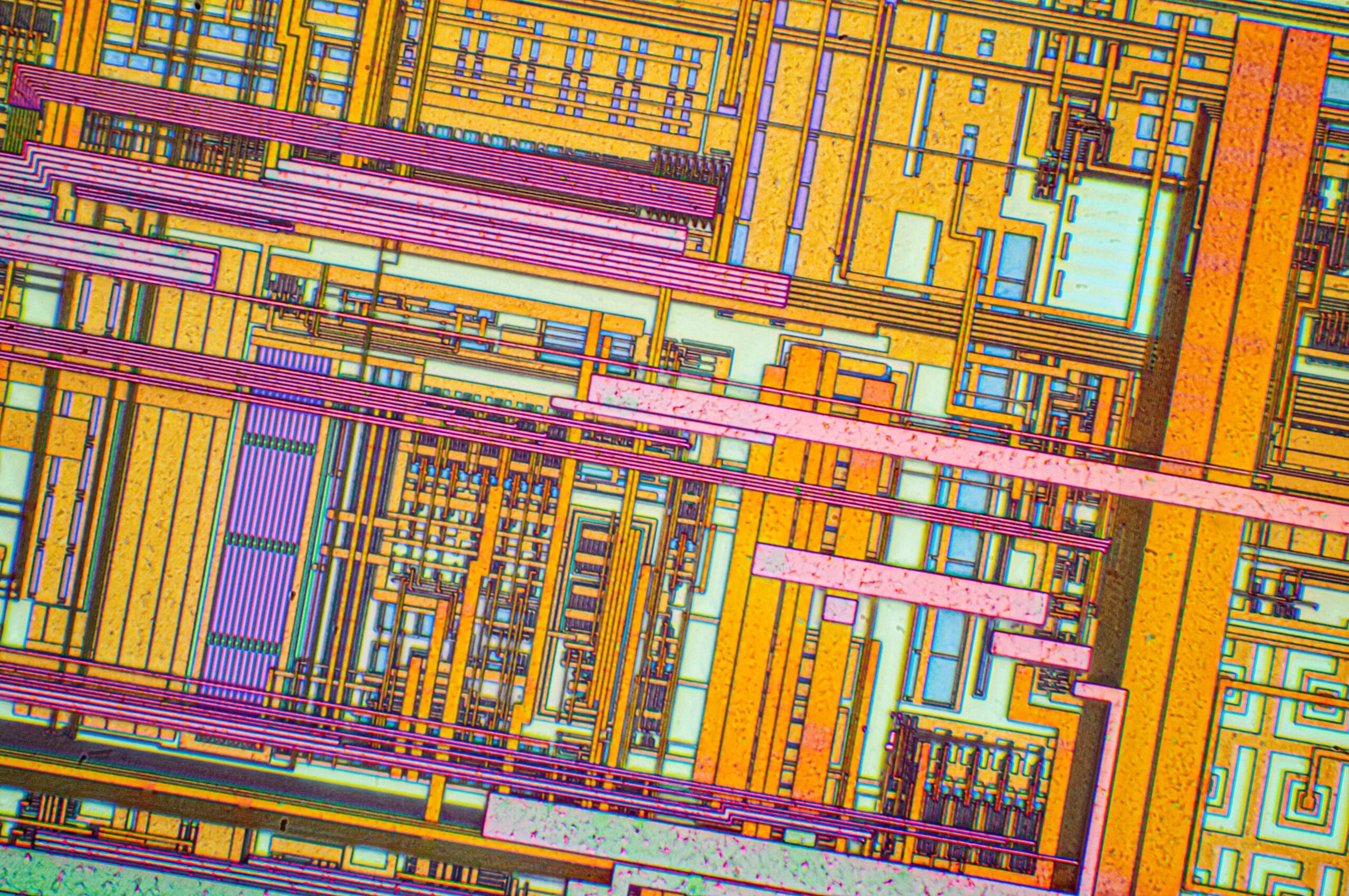
Image: Silicon chip from a computer laser mouse under a microscope 50х.jpg | File:Чип компьтерная мышь 50х.tif | License: CC BY-SA 4.0 | Source: Wikimedia | https://commons.wikimedia.org/wiki/File:Silicon_chip_from_a_computer_laser_mouse_under_a_microscope_50%D1%85.jpg