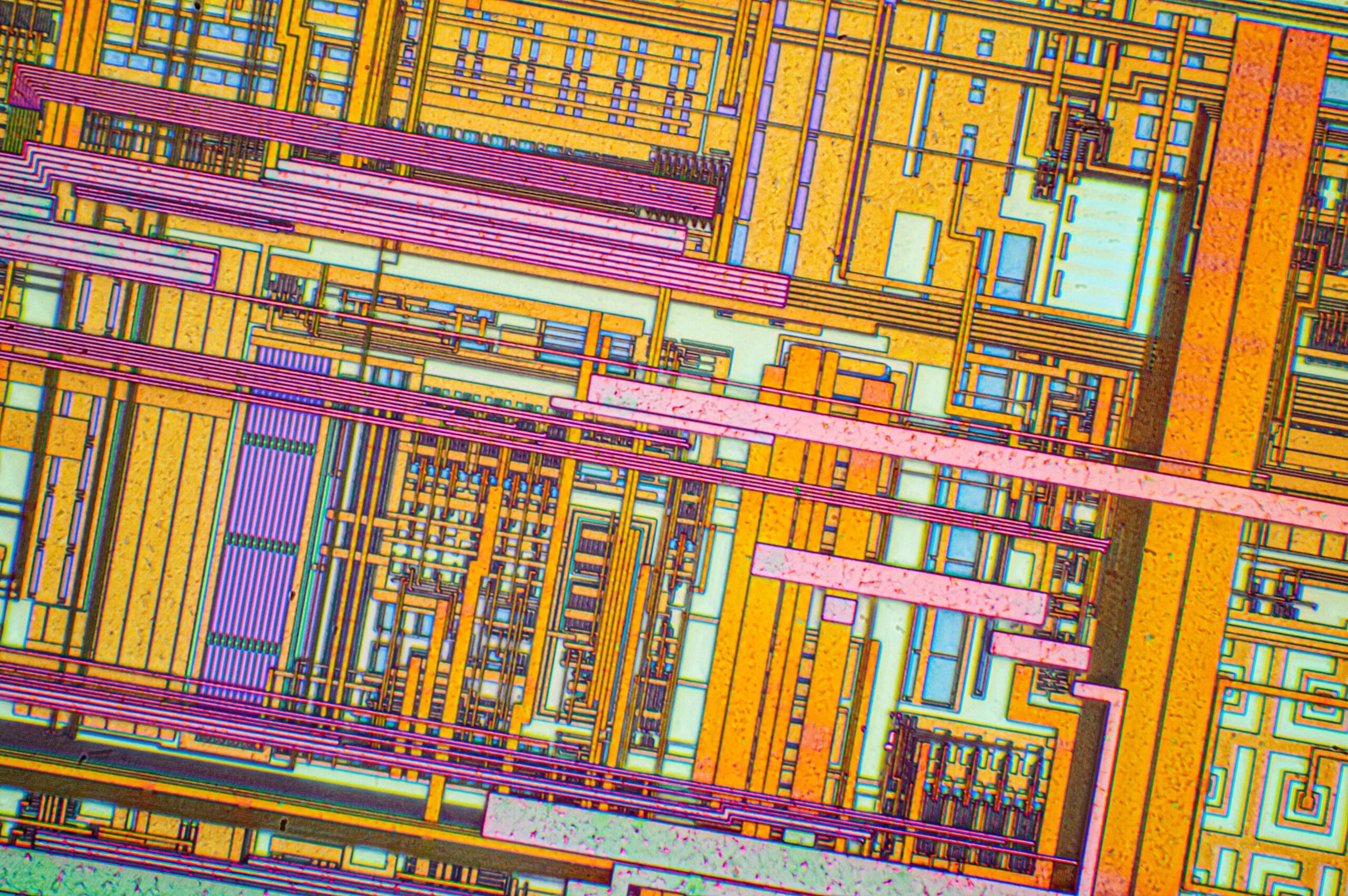
TSMC matters because modern computing increasingly depends on a company most consumers never see. The Taiwan Semiconductor Manufacturing Co. sits at the center of the semiconductor industry not as a brand-facing product company, but as the contract manufacturer that turns the designs of Apple, Nvidia, AMD, Qualcomm, Broadcom, and many others into physical chips. That role has become more consequential as advanced semiconductor production has turned into a narrow contest defined by lithography, yields, packaging, and capital intensity.
For years, the easiest shorthand for TSMC was that it made the world’s best chips. That is true, but incomplete. TSMC’s real advantage is operational: it runs a manufacturing system that lets customers design at the edge of what is physically possible while reducing the risk of failure, delay, or poor yield. In an industry where a small defect can erase billions of dollars in value, that reliability is not a side benefit. It is the product.
The company behind the bottleneck
TSMC is a pure-play foundry, which means it does not compete with most of its customers by selling branded chips of its own. That structure is central to its power. Designers can work with TSMC without worrying that the foundry is also trying to win the same end market with a competing processor. Over time, that neutrality has made TSMC the default home for companies that need leading-edge manufacturing but do not want to build and operate their own fabs.
The foundry model matters even more now because the cost of building a leading-edge fab has exploded. A modern facility can require tens of billions of dollars in equipment, clean-room infrastructure, process development, and ongoing upgrades. That capital burden creates a moat, but it also creates a trap for laggards: you can spend heavily and still fail to catch up if your process integration, yield learning, or supply-chain coordination is weaker than TSMC’s.
This is why competitive analysis around TSMC has to move beyond simple node naming. The battle is not just about whether a company can produce a chip at a certain process node. It is about whether it can produce that chip at scale, with acceptable defect rates, with enough packaging capacity, and with a predictable timeline that allows hyperscalers, device makers, and GPU vendors to plan product launches.
Why advanced node leadership still decides the market
The semiconductor industry has spent years talking about nodes such as N5, N3, and future-class processes. The labels themselves can be more marketing than measurement, but the strategic reality is straightforward: smaller and more advanced process technologies usually deliver better performance, better power efficiency, or more transistors in the same area. For AI accelerators, smartphone SoCs, and high-end CPUs, those gains matter because the limiting factors are now often power and packaging density rather than raw design ambition.
TSMC’s lead on advanced nodes gives its customers a practical advantage. Apple can squeeze more performance per watt into mobile devices. Nvidia can build denser accelerators for data centers. AMD can compete more aggressively in CPUs and GPUs. The foundry does not design the winning product, but it defines the manufacturing envelope in which the winning product can exist.
That is why TSMC’s importance has intensified alongside AI. Modern AI systems are not powered by a single chip. They are assembled from CPUs, GPUs, networking silicon, memory, and increasingly specialized accelerators, all of which must fit into an intricate manufacturing and packaging pipeline. The companies winning in AI hardware are often the ones that can secure enough leading-edge wafers and enough advanced packaging capacity to turn a theoretical design into a shipped system.
The packaging story is as important as the transistor story
One of the biggest misunderstandings in semiconductor coverage is treating the wafer fab as the whole story. In AI and high-performance computing, packaging has become a major constraint in its own right. TSMC’s advanced packaging technologies, especially its CoWoS platform, have become strategically important because they allow chiplets, high-bandwidth memory, and large accelerators to be integrated into performance-critical systems.
This matters because the old assumption that one monolithic die is the best way to build a chip is no longer always true. Large dies become difficult to manufacture at good yields. Splitting a design into chiplets can improve economics and flexibility. But chiplets only help if the interconnect, packaging, and testing infrastructure are mature enough to keep latency and reliability under control.
TSMC has made packaging a core part of its manufacturing proposition rather than a back-end afterthought. That gives it leverage in the AI supply chain. When GPU demand surges, the constraint is not simply “can someone etch the silicon?” It is “can the chip be packaged, tested, and delivered in enough volume to satisfy data center buyers?” The answer is often no unless the customer is well positioned inside TSMC’s manufacturing queue.
Why rivals have struggled to close the gap
Intel, Samsung, and other rivals have all invested heavily in advanced semiconductor manufacturing. Yet TSMC remains the benchmark because semiconductor leadership depends on repeated execution, not a single breakthrough. Process technology is cumulative. Yield learning compounds over time. The supplier ecosystem, the design tool flow, the customer trust, and the fab cadence all matter together.
Intel’s foundry ambitions are significant, but they are still in the process of proving that they can attract large external customers at scale while maintaining competitiveness in cost, performance, and schedule. Samsung has advanced manufacturing capabilities, but it has faced a more uneven reputation in leading-edge foundry execution. Other players, including foundry specialists in China and elsewhere, do not yet offer the same combination of scale, technical depth, and ecosystem confidence at the cutting edge.
TSMC’s advantage is therefore not merely a single process node lead. It is the trust of customers who need billions of dollars of chips to arrive on time and work as expected. In semiconductors, that trust is brutally hard to earn and easy to lose.
The economics of being indispensable
TSMC’s business model is unusually elegant for an industry as physically demanding as chipmaking. Customers fund design; TSMC absorbs the manufacturing complexity; the company then monetizes scale, yield, and process leadership. The more advanced the node, the more valuable the manufacturing slot becomes. That creates a powerful economic flywheel: leading customers bring leading designs, which justifies more capital spending, which improves the process, which attracts more customers.
But the economics are not risk-free. Capital expenditures are enormous and cyclical. Demand can shift quickly. Geopolitical risk is real. And the cost of standing still is severe, because competitors are also trying to move up the curve. A foundry can be profitable and still vulnerable if its lead starts to narrow faster than customers can diversify.
TSMC’s pricing power is strongest where alternative capacity is weakest. That is why AI-related demand has become so important. High-performance accelerators are expensive chips with large margins, which gives foundries room to invest in the most difficult manufacturing steps. Yet the same chips also intensify dependency, because customers cannot easily swap to another supplier without redesigning the product, changing the software stack, and accepting schedule risk.
Why Taiwan is part of the company’s strategy
Any honest analysis of TSMC has to address geography. The company’s manufacturing base in Taiwan is not just a corporate detail; it is a strategic factor for the entire global tech industry. Taiwan’s semiconductor cluster offers dense talent, supplier relationships, and decades of manufacturing experience. Those advantages help explain why TSMC is so hard to duplicate elsewhere.
At the same time, geographic concentration raises obvious resilience questions. Customers, governments, and investors all understand that advanced chip supply is now intertwined with cross-strait tension, export controls, industrial policy, and national security concerns. TSMC has responded with diversification efforts, including overseas fabs, but moving advanced manufacturing is not like copying a factory blueprint. It requires reproducing an ecosystem of tools, materials, process knowledge, and skilled labor.
That is why policy discussions around TSMC often miss the central point. The issue is not only where the company builds fabs. It is whether any other region can reproduce the full manufacturing stack at comparable scale and quality. So far, no one has demonstrated that capability at the leading edge.
What TSMC means for AI, GPUs, and data centers
TSMC’s influence is easiest to see in the AI supply chain. The explosive demand for data center GPUs and other accelerators has put extraordinary pressure on advanced wafer capacity and packaging. Companies building AI infrastructure are not just buying chips; they are competing for a scarce manufacturing pipeline that includes wafer starts, interconnects, substrates, high-bandwidth memory integration, and final test.
For cloud operators and enterprise buyers, this changes procurement strategy. Hardware availability becomes a planning variable. Product launch dates depend on manufacturing queues. Infrastructure buildouts can be slowed by packaging bottlenecks even when demand is strong. TSMC therefore functions as a hidden scheduler of the global AI economy.
The same dynamic applies outside AI. Smartphones, automotive electronics, networking gear, and consumer devices all depend on semiconductor supply chains that TSMC helps anchor. The company’s decisions on capacity, technology transition, and packaging expansion ripple outward into retail launches, carrier upgrades, factory automation, and industrial equipment.
The bigger competitive picture
What makes TSMC the world’s most important chip company is not that it has eliminated competition. It is that the rest of the industry still has to organize itself around TSMC’s capabilities. Nvidia designs around TSMC. Apple plans around TSMC. Rivals compare themselves to TSMC. Governments court TSMC. Investors watch TSMC for clues about the health of advanced computing demand.
That centrality is unlikely to disappear soon. Even if competitors narrow the gap, the combination of process leadership, packaging strength, scale, and customer trust is self-reinforcing. In semiconductor manufacturing, small advantages become strategic because they are multiplied across billions of transistors and thousands of wafers. TSMC has spent decades turning that compounding effect into a durable business model.
The result is a company that rarely appears in consumer conversations but shapes almost every major computing platform underneath them. In the AI era, that role has only become more visible. The companies that design the chips get the headlines. The company that makes them possible still holds the stronger position.
Sources and further reading
- TSMC Annual Reports and quarterly earnings materials
- TSMC Technology Symposia presentations
- U.S. Congressional Research Service semiconductor supply chain reports
- ASML annual reports and investor presentations for lithography context
- Intel, Samsung Foundry, and TSMC public roadmaps and investor materials
- Industry analyses from SEMI and major semiconductor trade publications
Image: Silicon chip from a computer laser mouse under a microscope 50х.jpg | File:Чип компьтерная мышь 50х.tif | License: CC BY-SA 4.0 | Source: Wikimedia | https://commons.wikimedia.org/wiki/File:Silicon_chip_from_a_computer_laser_mouse_under_a_microscope_50%D1%85.jpg